基于水平微米线阵列的CVD石墨烯周期性应变研究
doi: 10.11951/j.issn.1005-0299.20250077
张琳 , 尹涵 , 李云爻 , 高雪娇
华北电力大学(保定) 数理系河北省物理学与能源技术重点实验室,河北 保定 071003
基金项目: 华北电力大学青年人才引育项目(20226942).
Horizontal microwires array enabled periodic strain in CVD graphene
ZHANG Lin , YIN Han , LI Yunyao , GAO Xuejiao
Hebei Key Laboratory of Physics and Energy Technology, Department of Mathematics and Physics, North China Electric Power University, Baoding 071003 , China
摘要
针对在化学气相沉积(Chemical Vapor Deposition,CVD)石墨烯上难以施加周期性应变的问题,对湿法转移过程进行了优化,并分析了微米线高度对应变的影响。首先,通过延长铜基底刻蚀时间、提高目标衬底洁净度、旋涂均匀的PMMA覆盖层等方法优化了CVD石墨烯湿法转移过程,使得石墨烯上的破损显著减少且可重复性高。其次,使用优化后的湿法转移技术将CVD石墨烯转移至不同高度的水平微米线上。最后,利用光学显微镜和微区拉曼快速成像对石墨烯的形貌以及质量进行了表征分析。研究结果表明,水平微米线间隔处的CVD石墨烯上产生明显的周期性拉应变,单轴拉应变值受到水平微米线高度的影响:30、285 nm高的微米线分别对石墨烯施加了0.16%、0.54%的单轴拉应变,而560 nm高的微米线则导致微米线间隔处的石墨烯普遍发生断裂。该结果对于二维材料的周期性应变工程具有参考价值。
Abstract
To apply periodic strain on chemical vapor deposition (CVD) graphene, the wet transfer process was optimized, and the influence of the height of the microwires on the strain was analyzed. First, the wet transfer process for CVD graphene was optimized by increasing the etching time of copper substrate, improving the cleanness of target substrate, and coating a uniform PMMA layer. As a result, the cracks on the transferred graphene were significantly reduced, and reproducibility improved. Secondly, CVD graphene was transferred onto horizontal microwires array of different heights using the optimized wet transfer method. Finally, the morphology and quality of graphene were characterized via an optical microscope and micro-area Raman rapid imaging. The relevant results showed that periodic tensile strain was generated on the CVD graphene at the intervals of horizontal microwires. The uniaxial tensile strain value was affected by the height of the horizontal microwires: the 30-nm-high and 285-nm-high microwires induced 0.16% and 0.54% uniaxial tensile strain to the graphene, respectively, while the 560-nm-high microwires caused widespread cracks on the graphene at the intervals of the microwires. These results have reference value for periodic strain engineering in 2D materials.
石墨烯是由单层碳原子以sp2杂化形成的二维材料,具有优异的力学性能。理论上石墨烯的杨氏模量约为1 TPa,理论抗拉强度高达130 GPa,是已知最强的材料之一 [1-2]。可以通过大范围的改变石墨烯上的应变,有效调控石墨烯的力学[2]、电学[3]、光学[4]和热学性能[5]。在电学性能方面,石墨烯上的应变可以改变费米面和费米速度的各向异性,进而影响电导率[6]。沿锯齿方向施加≥20%应变时,有望打开带隙,使石墨烯从半金属向半导体转变[7]。与摩尔超晶格技术配合使用,施加0.35%的应变即可有效调控能带结构,在石墨烯上打开带隙[8-9]。由此可见,石墨烯的应变调控研究对于发展石墨烯应变电子学具有重要意义。
化学气相沉积(Chemical Vapor Deposition,CVD)是大规模生长石墨烯的主要方法[10]。通过CVD合成能够获得厘米尺度、覆盖率达到95%以上的高质量单层石墨烯。然而生长过程中,通常在铜箔、镍箔等金属衬底上进行催化。在使用时,需要把石墨烯转移到目标衬底上。大面积的石墨烯转移方法包括湿法转移[10-11]、干法转移[12-13]、鼓泡法[14-15]、准干转移[16-17]、卷对卷转移[18],其中湿法转移利用化学溶液刻蚀掉石墨烯的铜基底,再通过聚甲基丙烯酸甲酯(PMMA)支撑层将石墨烯转移到目标基底上,适合用于大规模转移CVD石墨烯。
优化湿法转移工艺、减少转移造成的破损以及有机残留是保持石墨烯力学、电学性能的关键,也是近年来的研究热点。具体的优化方向包括:增强覆盖层与石墨烯的接触,加大保护作用[19];增强石墨烯与目标衬底的接触,缓解来自液体的张力[20];清洗过程中降低溶剂表面张力[21];让表面张力均匀作用[22]等途径。
在石墨烯上施加应变的常见方法包括机械拉伸法[23-24]、弯曲柔性衬底法[25-26]、热膨胀法[27],以及纳米结构支撑法[28-29]。其中,纳米结构支撑法适合大规模施加周期性应变。将石墨烯转移到纳米柱[30]、纳米孔[31]等微结构上,通过局部弯曲或拉伸引入应变。并且,可以通过控制几何形状和尺寸,改变石墨烯的局部受力状态,进而调控应变。
本文首先对石墨烯的湿法转移中出现的多层石墨烯残留、铜基残留、PMMA覆盖层旋涂不均匀以及衬底杂质颗粒导致的破损等问题进行优化。然后,使用优化后的湿法转移技术将CVD石墨烯转移至水平微米线阵列上。随后,应用微区拉曼快速成像系统分析石墨烯G峰的拉曼位移。最后,应用水平微米线阵列在石墨烯上施加周期性的单轴拉应变,研究微米线的高度对石墨烯应变值的影响。
1 实验
使用的材料包括铜箔上生长的单层CVD石墨烯(泰州巨纳低维材料有限公司)、聚甲基丙烯酸甲酯溶液(PMMA 950 A4)、三氯化铁(FeCl3·6H2O,天津市大茂化学试剂厂)、丙酮(分析纯,天津市科密欧化学试剂有限公司)、无水乙醇(分析纯,天津市科密欧化学试剂有限公司)、单面抛光的SiO2/Si晶圆(100晶向,SiO2厚度285 nm,广州方岛半导体有限公司)。
石墨烯的湿法转移过程主要包括旋涂覆盖层、去除背面石墨烯、铜箔腐蚀、基底附着、去除覆盖层5个基本步骤,如图1所示。
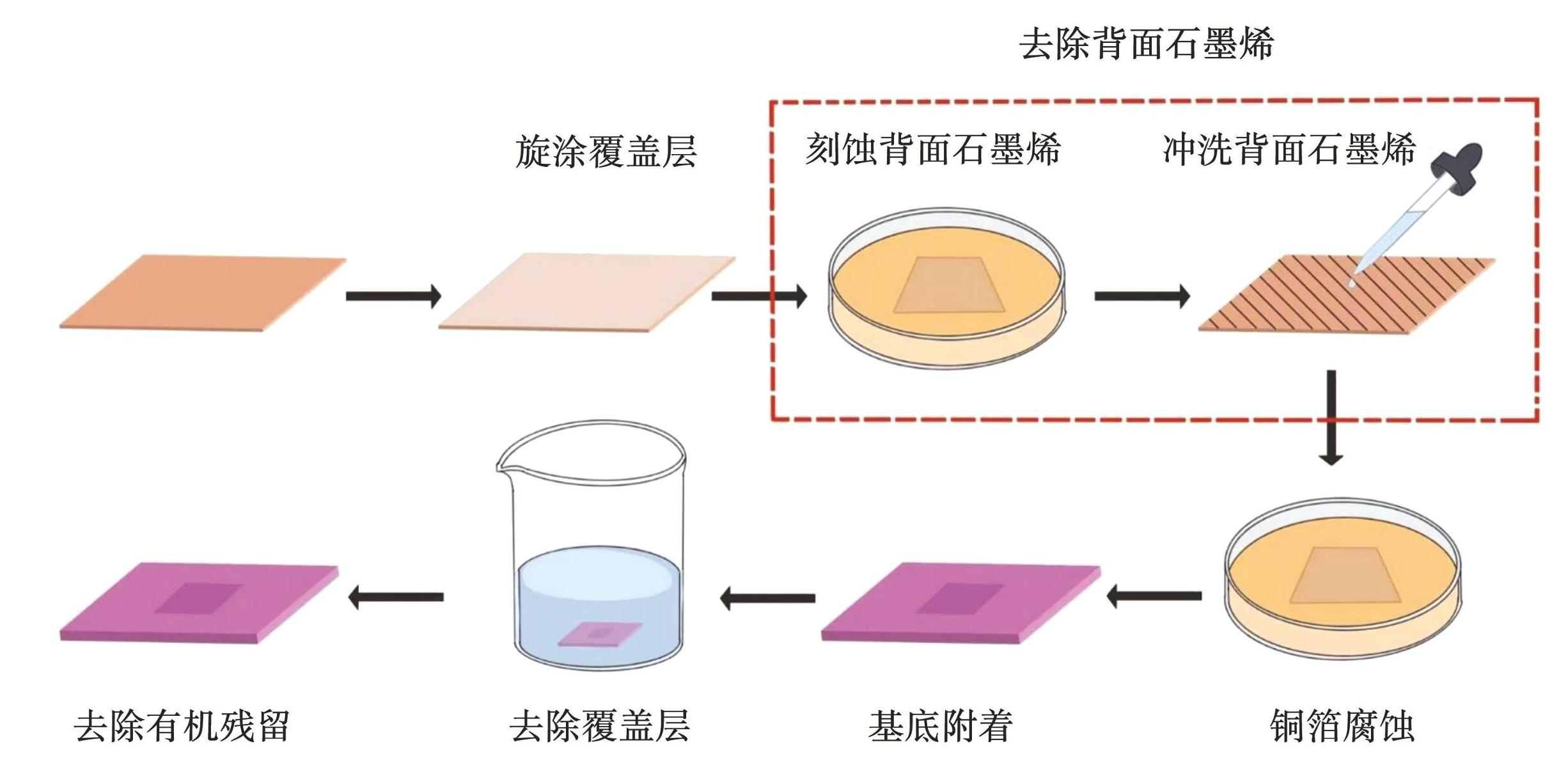
图1CVD石墨烯湿法转移的主要流程图
Fig.1Schematic illustration of main stepsin the wet transfer process for CVD graphene
具体操作流程包括:首先,将PMMA 950 A4在4 000 r/min,30 s的条件下旋涂于铜基CVD石墨烯表面,得到200 nm的PMMA覆盖膜;随后,将覆盖有PMMA的铜基石墨烯浸入0.1 mol/L的FeCl3刻蚀液中10 min,使用去离子水对石墨烯的背面进行彻底冲洗,以清除背面石墨烯(也可以使用氧等离子体去除);继续在FeCl3溶液中刻蚀4 h,以充分溶解铜基底;接下来,将PMMA支撑的石墨烯附着到目标基底上;最后,使用丙酮溶液去除石墨烯上的PMMA 覆盖层,完成石墨烯的湿法转移。这个过程常伴随着石墨烯的破损和有机残留,直接影响石墨烯的应变调控。因此,有必要分析具体原因,并对湿法转移进行优化。
将石墨烯转移到垂直纳米线、垂直三棱锥上时往往会引入褶皱,使应变复杂[32]。通过紫外光刻和BOE(VNH4F∶VHF=6∶1)湿法刻蚀在SiO2/Si衬底上制备水平微米线阵列。水平微米线宽度约5 μm,间隔约5 μm,高度分别为30和285 nm,结构如图2所示。预期能够施加单轴拉应变,同时不产生褶皱。
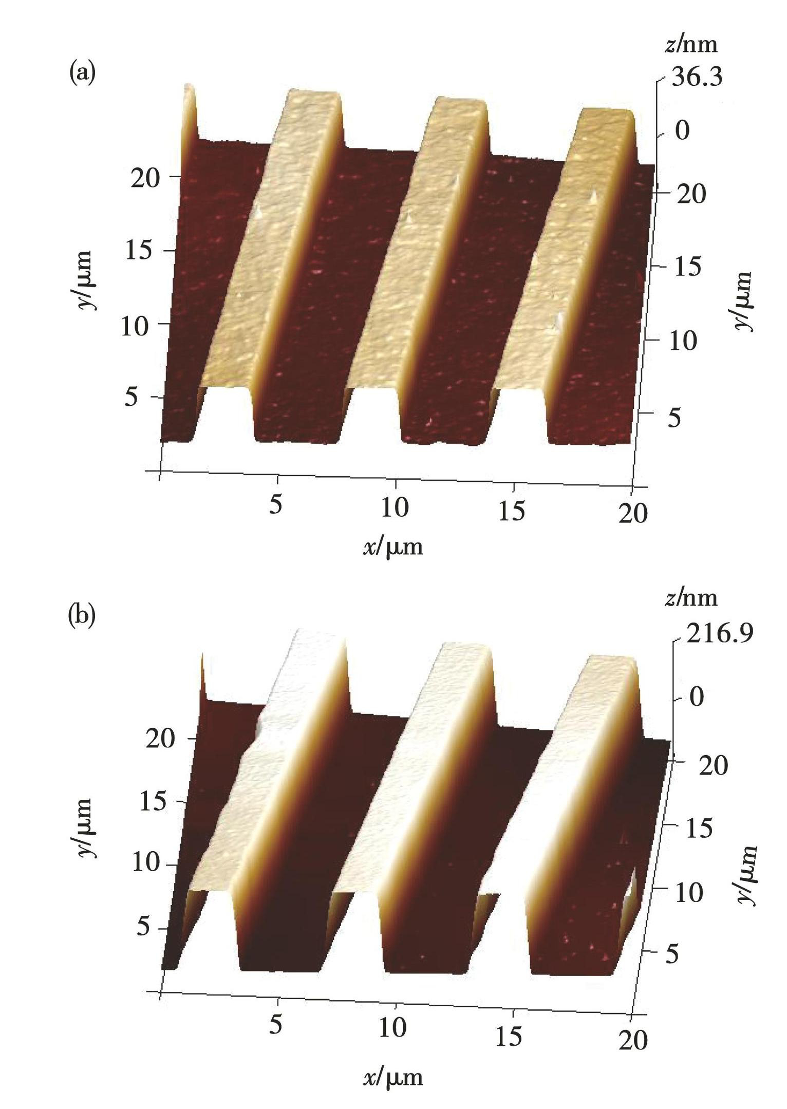
图2水平微米线的AFM图像:(a)30 nm高微米线阵列;(b)285 nm高微米线阵列
Fig.2AFM images of horizontal microwires: (a) 30 nm microwires; (b) 285 nm microwires
在石墨烯的化学气相沉积过程中,会形成不同大小和形状的晶粒(如图3(a)所示)。多晶石墨烯的晶粒尺寸和质量直接影响石墨烯的力学性能。收集了10个样品在100倍下的光学图像,通过数格子法对晶粒的面积进行了统计分析。结果显示,晶粒面积在1×10⁴~5×104 μm2范围内的数量最多(如图3(b))。整个CVD石墨烯上,≥1×104 μm2的晶粒占据了整个面积的96%(如图3(c)),<1×104 μm2的晶粒只占整个面积的4%。根据统计结果,绝大多数晶粒能够完全覆盖微米线的宽度和间隙,因此在后续应变分析中,多数情况可以不考虑晶界影响。
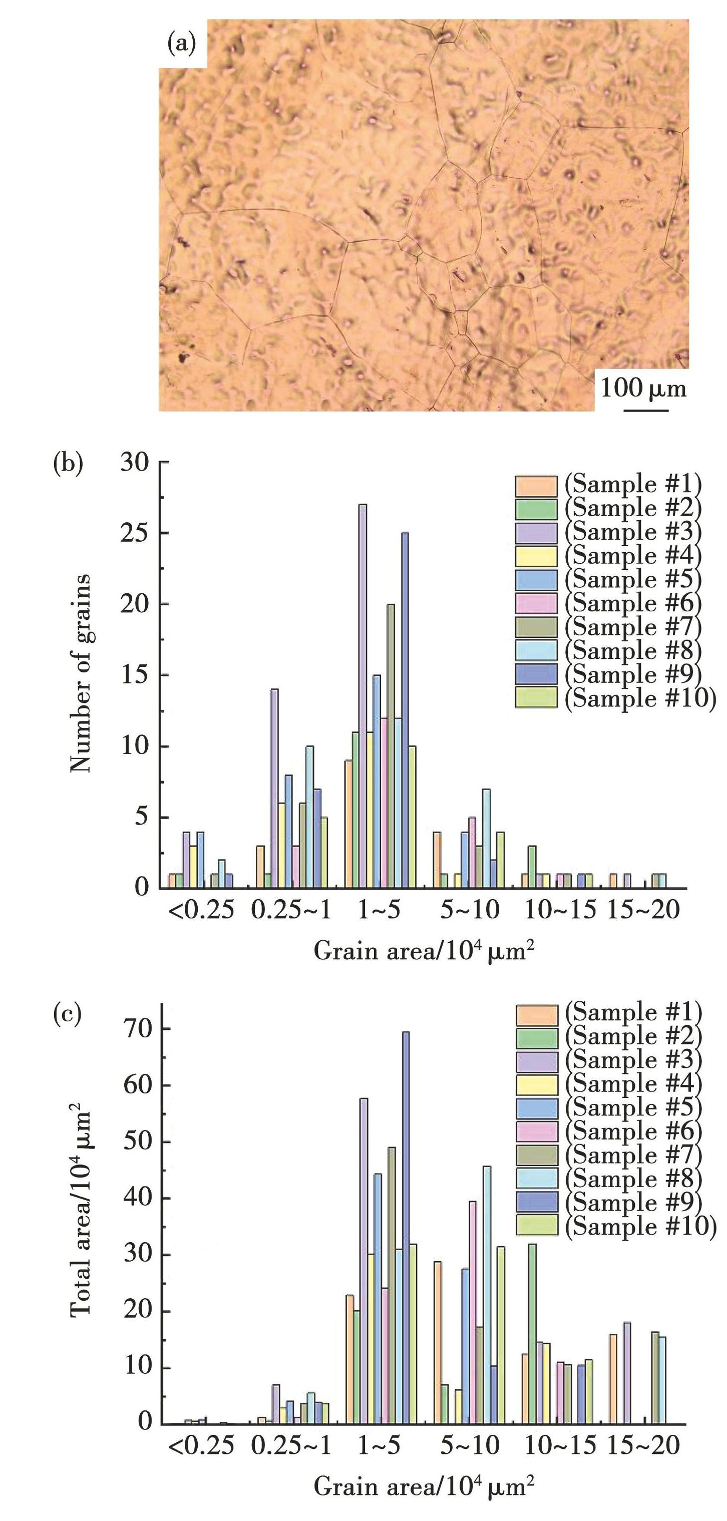
图3(a)铜箔上CVD生长的单层多晶石墨烯的光学图以及不同尺寸晶粒的数目(b)和面积(c)统计图
Fig.3(a) Optical image of single-layer polycrystalline graphene grown by CVD on copper foil and statistical graphs of the number (b) and total area (c) of grains with different sizes
2 结果与分析
2.1 湿法转移优化
在石墨烯的湿法转移过程中,遇到以下几个方面的问题。首先,转移后的石墨烯表面出现类似多层石墨烯的区域(图4(a)中红色圆圈所示),这是背面石墨烯清洗不彻底导致的。用去离子水彻底冲洗背面可以完全消除(图4(b));图4(c)中红色圆圈所示黑色团聚颗粒物是铜箔刻蚀时间不充分(1 h)导致的金属铜残留,适当延长刻蚀时间至4 h后黑色颗粒消失(图4(d))。在1 500 r/min、20 s旋涂条件下PMMA的厚度约300 nm,太厚或不均匀会造成清洗过程中张力不均匀,进而产生大面积的破损(图4(e)),均匀旋涂200 nm的PMMA覆盖层,能够有效解决这个问题,消除大面积破损(图4(f))。最后,转移的CVD石墨烯出现大尺寸破洞(图4(g)中红色圆圈所示),这与目标衬底表面的杂质颗粒有关,通过传统RCA(Radio Corporation of America)清洗去除衬底表面颗粒,能够避免产生大尺寸破洞(图4(h))。
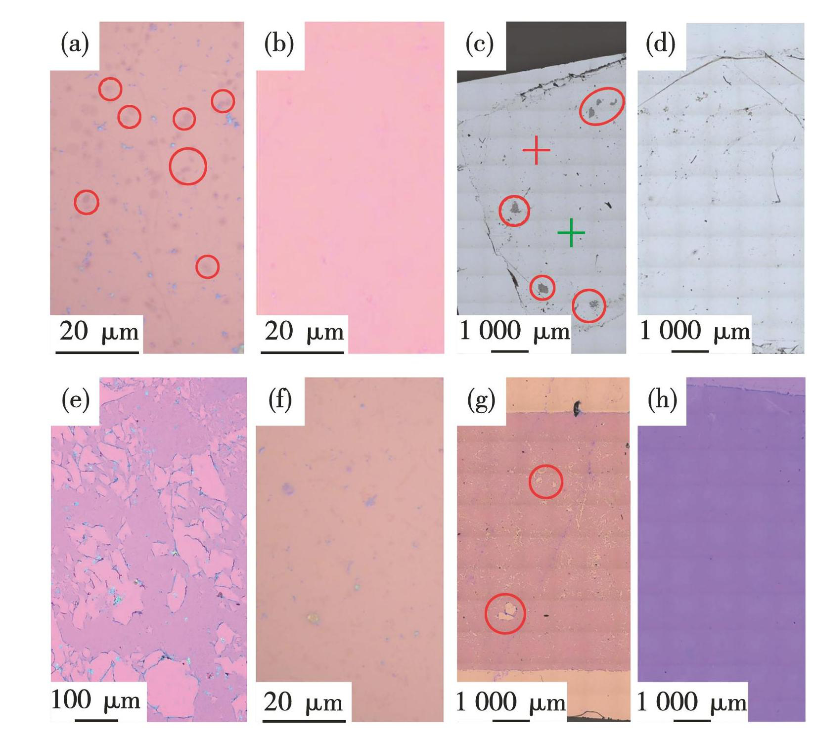
图4湿法转移过程中的常见问题及优化结果:(a)背面石墨烯残留及(b)去离子水冲洗优化;(c)铜基残留及(d)优化;(e)石墨烯破损及(f)优化;(g)石墨烯大尺寸破洞及(h)优化
Fig.4Common problems and optimization results in the process of wet transfer: (a) residue of backside graphene and optimization results by a complete deionized water rinsing on the backside (b) ; (c) copper residue and optimization results (d) ; (e) graphene cracks and optimization results (f) ; (g) large-size holes in CVD graphene and optimization results (h)
针对以上4个方面进行优化后,湿法转移的CVD石墨烯更加洁净、完整。在光学显微镜下(图5(a))无明显的破损和有机残留。微区拉曼光谱(图5(b))显示出石墨烯的两个特征峰,在1 588 cm-1处的G峰和2 680 cm-1的2D峰[10,19],并且2D峰的强度大约是G峰的2倍,证明了石墨烯的单层结构。在1 345 cm-1处观察到缺陷峰D峰。D峰强度相比G峰强度较低,证明CVD石墨烯中含有少量缺陷。在PMMA做覆盖层的湿法转移研究中[15],这种方法以简单的步骤实现了石墨烯的无损转移。
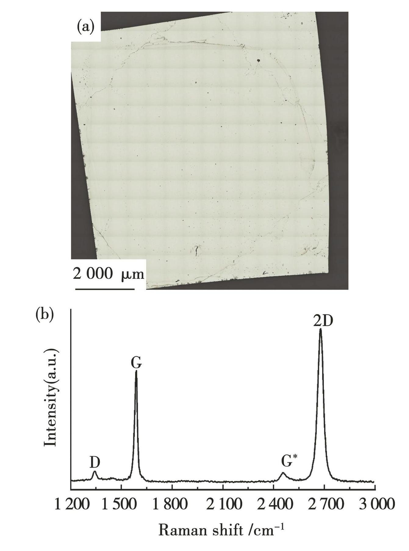
图5湿法转移优化后获得的单层石墨烯(a)及其拉曼光谱图(b)
Fig.5(a) Neat and complete single-layer grapheneby an optimized wet transfer process; (b) raman spectrum of graphene in fig. (a)
2.2 石墨烯上周期分布的单轴拉应变
使用优化后的湿法转移工艺将石墨烯转移到具有水平微米线阵列的衬底上(如图6所示)。衬底上的微米线结构对石墨烯施加单轴拉应变。石墨烯G峰是由碳原子的面内伸缩振动引起的,对所受的应力非常敏感。应用拉曼光谱快速成像技术测试石墨烯G峰的位移,进而分析应变大小和分布。
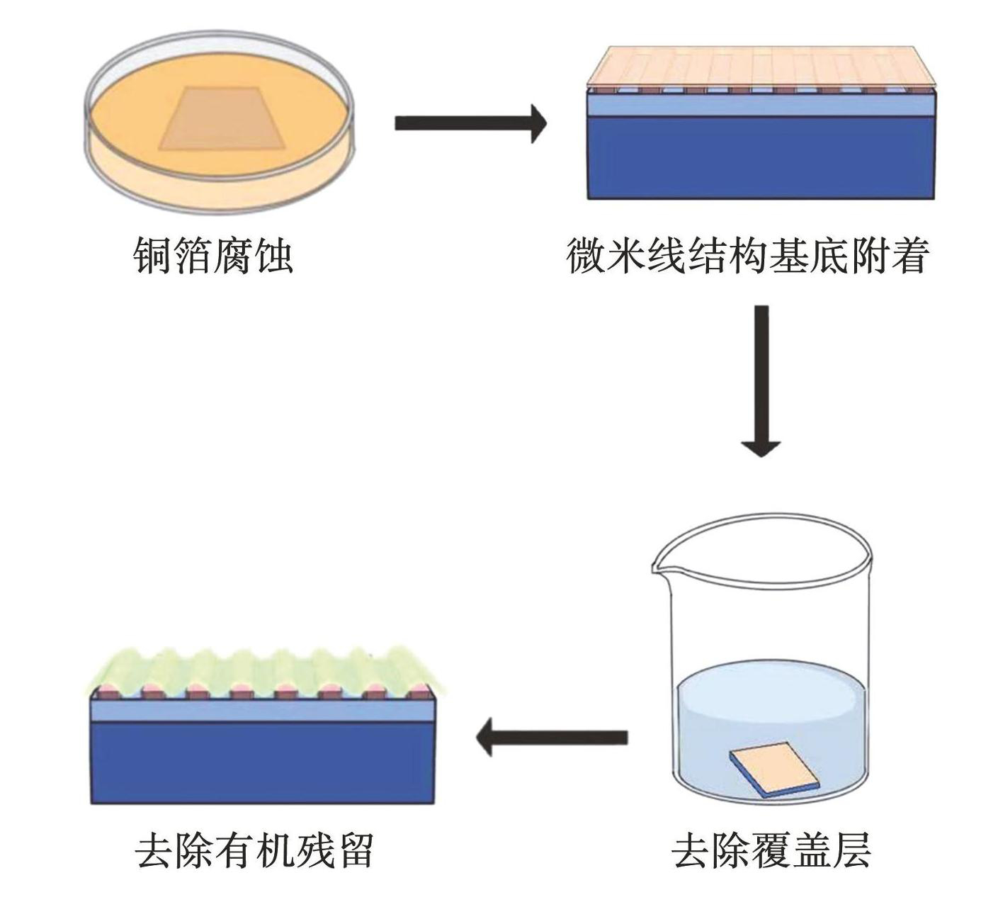
图6CVD石墨烯附着到微米线阵列上的示意图
Fig.6Schematic illustration of transferring CVD graphene to microwires array
图7、图8给出了不同高度微米线阵列上石墨烯的形貌以及应变变化情况。图7(a)和图8(a)中的光学图像中紫色区域为微米线,黄色区域为微米线的间隔。从图中可见,转移后的石墨烯无明显的破损与褶皱。
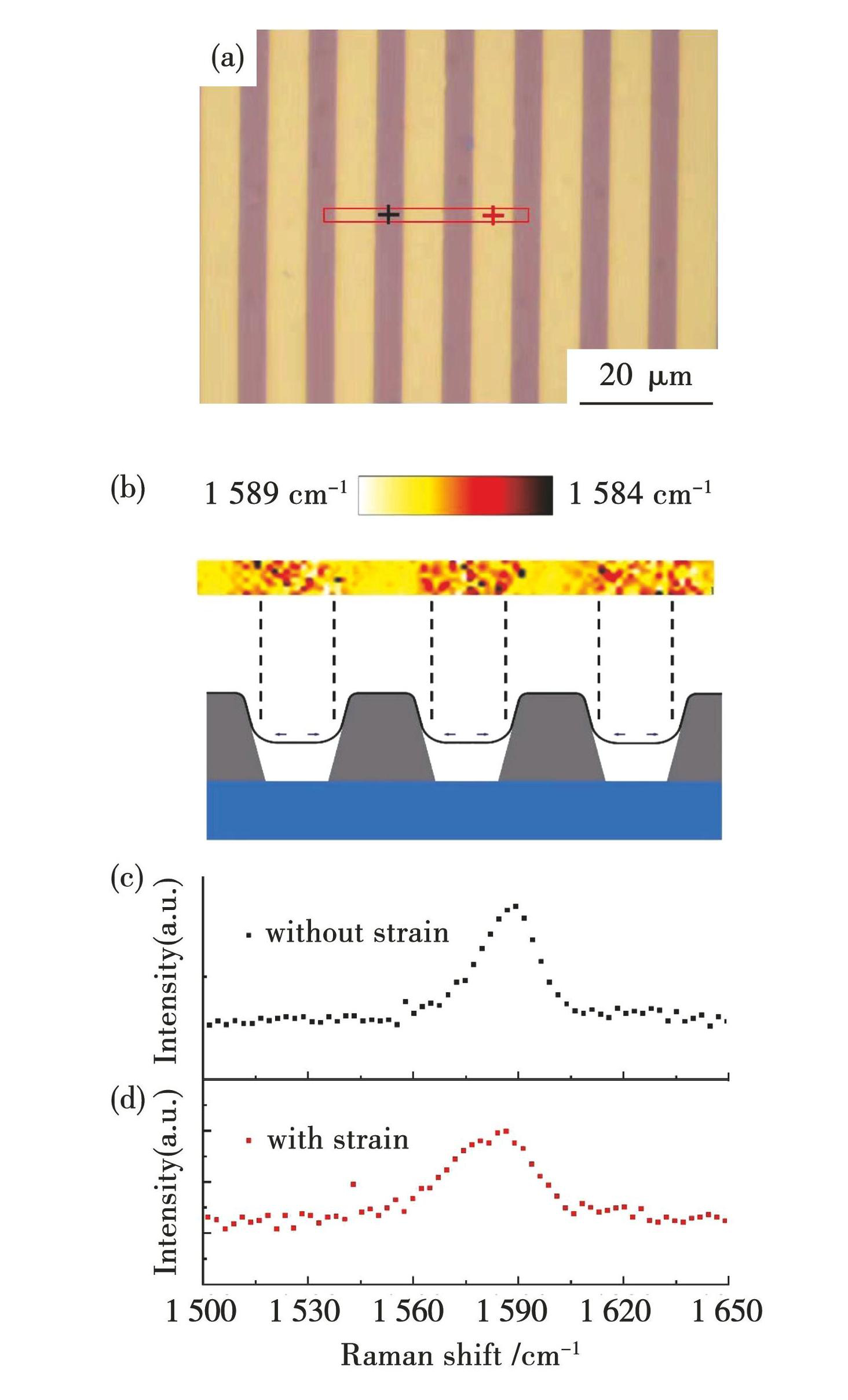
图730 nm高水平微米线阵列上石墨烯的应变情况:(a)CVD石墨烯的光学图;(b)图(a)中红色方块处石墨烯拉曼G峰位移分布图;(c)图(a)中黑色十字处未被单轴拉伸的石墨烯的拉曼G峰谱图;(d)图(a)中红色十字处被单轴拉伸的石墨烯的拉曼G峰谱图
Fig.7Strained graphene on 30-nm-high microwires array: (a) optical image of CVD graphene; (b) gra-phene G peak mapping in the red rectangular in fig.7 (a) ; (c) raman G peak spectrum of unstrained graphene at the black cross in fig.7 (a) ; (d) raman G peak spectrum of strained graphene at the red cross in fig.7 (a)
图7(b)~(d)为微米线阵列高度为30 nm时石墨烯的应变变化情况。对图7(a)中红色方框区域进行石墨烯G峰的二维扫描成像,得到图7(b)所示的拉曼位移分布图。在图7(a)黑色十字处提取的拉曼谱线显示G峰在1 589 cm-1,半高宽为18 cm-1(如图7(c)所示)。红色十字处提取的拉曼谱线显示G峰在1 584 cm-1处,半高宽为27 cm-1(如图7(d)所示)。其中黄色间隔区域对应的石墨烯G峰相比紫色微米线产生5 cm-1红移,表示这个区域的石墨烯受到拉应变作用。根据G峰应变位移系数-31.7 cm-1/%[33],单轴拉应变的值约为0.16%。此外,通过2D峰的位移计算的应变值为0.14%,与G峰的位移计算结果基本一致。根据微米线的几何结构判断应变为垂直于微米线方向的单轴应变。
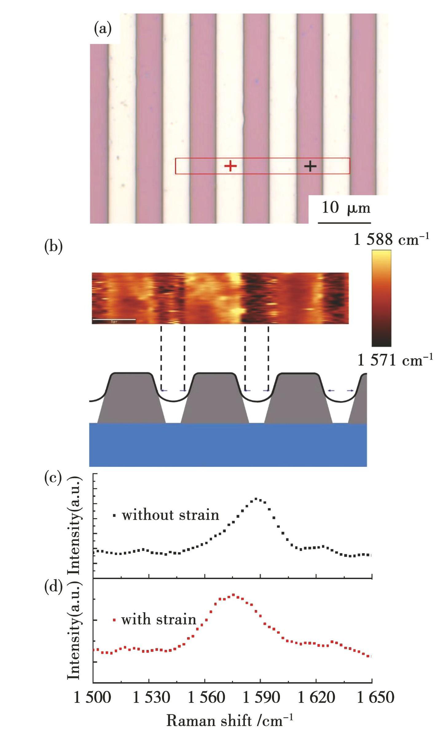
图8285 nm高水平微米线阵列上石墨烯的应变情况:(a)CVD石墨烯的光学图;(b)图(a)中红色方块处石墨烯拉曼G峰位移分布图;(c)图(a)中黑色十字处未被单轴拉伸的石墨烯的拉曼G峰谱图;(d)图(a)中红色十字处被单轴拉伸的石墨烯的拉曼G峰谱图
Fig.8Strained graphene on 285-nm-high microwires array: (a) optical image of CVD graphene; (b) gra-phene G peak mapping in the red rectangular in fig.8 (a) ; (c) raman G peak spectrum of unstrained graphene at the black cross in fig.8 (a) ; (d) raman G peak spectrum of strained graphene at the red cross in fig.8 (a)
图8(b)~(d)为微米线阵列高度为285 nm时石墨烯的应变变化情况。对图8(a)中红色方框区域做石墨烯G峰的二维扫描成像,得到图8(b)所示的拉曼位移分布图。其中黄色间隔区域对应的石墨烯G峰相比紫色微米线产生明显红移,表明在黄色间隔区域同样受垂直于微米线方向的拉伸作用,发生单轴应变。
在图8(a)黑色十字处提取的拉曼谱线显示G峰在1 588 cm-1,半高宽为26 cm-1(如图8(c)所示)。红色十字处提取的拉曼谱线显示G峰在1 571 cm-1处,半高宽为33 cm-1(如图8(d)所示)。在石墨烯受拉伸后,G峰左移17 cm-1并且半高宽变宽。根据G峰应变位移系数-31.7 cm-1/%[33],单轴拉应变的值约为0.54%。此外,通过2D峰的位移计算的应变值为0.52%,与G峰的位移计算结果基本一致。
图9为560 nm高的水平微米线阵列上石墨烯的形貌,可见,在微米线间隙处的石墨烯出现明显的条状裂纹,应变消失。裂纹的大小及分布呈现非均匀性,由此推测在CVD石墨烯上存在应力集中的点,裂纹以此为起点,随后大致沿着微米线的方向延伸。通过对比30、285和560 nm微米线阵列施加应变的结果发现,单轴拉应变的大小随微米线高度的增加而增大,到560 nm时产生明显裂纹,应变消失。此外,30 和285 nm微米线施加应变时,单轴拉应变都出现在石墨烯间隔处,由此推断它们的应变施加机理是一致的。石墨烯转移时,在水的毛细作用力下对石墨烯进行拉伸变形[34],最终通过石墨烯和SiO2间的摩擦力保持住变形。
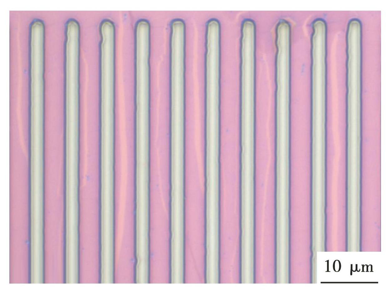
图9CVD石墨烯转移到560 nm高水平微米线阵列上的光学图
Fig.9Optical image of CVD graphene transferred onto 560 nm horizontal microwires array
3 结论
1)通过去除背面石墨烯残留、铜基残留、表面杂质颗粒,提高PMMA覆盖层的均匀性,显著提高了湿法转移CVD石墨烯的质量和可重复性。
2)使用水平微米线阵列可以在微米线间隔处的石墨烯上施加单轴拉应变,且不会产生褶皱。
3)CVD石墨烯上单轴拉应变的值与微米线高度有关,使用30、285 nm高的微米线时,微米线间隔处的石墨烯G峰分别发生5、17 cm-1的红移,对应0.16%与0.54%的单轴拉应变;当微米线高度增加至560 nm时,微米线间隔处的石墨烯普遍出现条状裂纹。
4)本文提出一种对石墨烯施加周期性应变的方法,并且操作过程可重复性高。相关结果为二维材料应变工程的规模化实施提供了可行的技术路径。
图1CVD石墨烯湿法转移的主要流程图
Fig.1Schematic illustration of main stepsin the wet transfer process for CVD graphene
图2水平微米线的AFM图像:(a)30 nm高微米线阵列;(b)285 nm高微米线阵列
Fig.2AFM images of horizontal microwires: (a) 30 nm microwires; (b) 285 nm microwires
图3(a)铜箔上CVD生长的单层多晶石墨烯的光学图以及不同尺寸晶粒的数目(b)和面积(c)统计图
Fig.3(a) Optical image of single-layer polycrystalline graphene grown by CVD on copper foil and statistical graphs of the number (b) and total area (c) of grains with different sizes
图4湿法转移过程中的常见问题及优化结果:(a)背面石墨烯残留及(b)去离子水冲洗优化;(c)铜基残留及(d)优化;(e)石墨烯破损及(f)优化;(g)石墨烯大尺寸破洞及(h)优化
Fig.4Common problems and optimization results in the process of wet transfer: (a) residue of backside graphene and optimization results by a complete deionized water rinsing on the backside (b) ; (c) copper residue and optimization results (d) ; (e) graphene cracks and optimization results (f) ; (g) large-size holes in CVD graphene and optimization results (h)
图5湿法转移优化后获得的单层石墨烯(a)及其拉曼光谱图(b)
Fig.5(a) Neat and complete single-layer grapheneby an optimized wet transfer process; (b) raman spectrum of graphene in fig. (a)
图6CVD石墨烯附着到微米线阵列上的示意图
Fig.6Schematic illustration of transferring CVD graphene to microwires array
图730 nm高水平微米线阵列上石墨烯的应变情况:(a)CVD石墨烯的光学图;(b)图(a)中红色方块处石墨烯拉曼G峰位移分布图;(c)图(a)中黑色十字处未被单轴拉伸的石墨烯的拉曼G峰谱图;(d)图(a)中红色十字处被单轴拉伸的石墨烯的拉曼G峰谱图
Fig.7Strained graphene on 30-nm-high microwires array: (a) optical image of CVD graphene; (b) gra-phene G peak mapping in the red rectangular in fig.7 (a) ; (c) raman G peak spectrum of unstrained graphene at the black cross in fig.7 (a) ; (d) raman G peak spectrum of strained graphene at the red cross in fig.7 (a)
图8285 nm高水平微米线阵列上石墨烯的应变情况:(a)CVD石墨烯的光学图;(b)图(a)中红色方块处石墨烯拉曼G峰位移分布图;(c)图(a)中黑色十字处未被单轴拉伸的石墨烯的拉曼G峰谱图;(d)图(a)中红色十字处被单轴拉伸的石墨烯的拉曼G峰谱图
Fig.8Strained graphene on 285-nm-high microwires array: (a) optical image of CVD graphene; (b) gra-phene G peak mapping in the red rectangular in fig.8 (a) ; (c) raman G peak spectrum of unstrained graphene at the black cross in fig.8 (a) ; (d) raman G peak spectrum of strained graphene at the red cross in fig.8 (a)
图9CVD石墨烯转移到560 nm高水平微米线阵列上的光学图
Fig.9Optical image of CVD graphene transferred onto 560 nm horizontal microwires array
NOVOSELOV K S, GEIM A K, MOROZOV S V,et al. Electric field effect in atomically thin carbon films[J]. Science,2004,306(5696):666-669. DOI:10.1126/science.1102896
CAO Ke, FENG Shizhe, HAN Ying,et al. Elastic straining of free-standing monolayer graphene[J]. Nature Communications,2020,11(1):284. DOI:10.1038/s41467-019-14130-0
GONG Tianxun, YU Mengya, LIU Zhenyi,et al. Strain engineering in monolayer graphene via ZnO array substrates in Schottky junction for enhanced optoelectronic performance[J]. Surfaces and Interfaces,2025,58:105859. DOI:10.1016/j.surfin.2025.105859
HASANIROKH K, NAIFAR A. Quantitative analysis on the optical kerr impact and third harmonic generation in beltrami-shaped curved graphene[J]. Scientific Reports,2025,15(1):1666. DOI:10.1038/s41598-025-85303-9
LI Wentao. Effect of biaxial strain on structural,electronic,and thermal transport properties of twin graphene: A comparative study with γ-graphyne[J]. Journal of Electronic Materials,2025,54(1):693-702. DOI:10.1007/s11664-024-11429-7
PRABHAKAR S, MELNIK R. First-principles calculations of electrical conductivities of edge-modified graphene nanoribbons: Strain effect[J]. Physica E: Low-dimensional Systems and Nanostructures,2022,142:115267. DOI:10.1016/j.physe.2022.115267
SHU Yu, HE Kaijun, XIONG Rui,et al. Strain engineering on the electronic properties and interface contact of graphene/GeN3 van der Waals heterostructure[J]. Applied Surface Science,2022,604:154540. DOI:10.1016/j.apsusc.2022.154540
HUDER L, ARTAUD A, LE QUANG T,et al. Electronic spectrum of twisted graphene layers under heterostrain[J]. Physical Review Letters,2018,120(15):156405. DOI:10.1103/PhysRevLett.120.156405
MEAPLE F, MISSAOUI A, CEA T,et al. Heterostrain determines flat bands in magic-angle twisted graphene layers[J]. Physical Review Letters,2021,127(12):126405. DOI:10.1103/PHYSREVLETT.127.126405
LI Xuesong, CAI Weiwei, AN Jinho,et al. Large-area synthesis of high-quality and uniform graphene films on copper foils[J]. Science,2009,324(5932):1312-1314. DOI:10.1126/SCIENCE.1171245
GAO Xin, ZHENG Liming, LUO Fang,et al. Integrated wafer-scale ultra-flat graphene by gradient surface energy modulation[J]. Nature Communications,2022,13(1):5410. DOI:10.1038/s41467-022-33135-w
HUANG Shiming, ZHU Lianying, ZHAO Yongxin,et al. Giant magnetoresistance induced by spin-dependent orbital coupling in Fe3GeTe2/graphene heterostructures[J]. Nature Communications,2025,16(1):2866. DOI:10.1038/s41467-025-58224-4
YOON Min-Ah, KIM Chan, KIM Jae-Hyun,et al. Surface properties of CVD-grown graphene transferred by wet and dry transfer processes[J]. Sensors(Basel),2022,22(10):3944. DOI:10.3390/s22103944
WANG M, YANG E H, VAJTAI R,et al. Effects of etchants in the transfer of chemical vapor deposited graphene[J]. Journal of Applied Physics,2018,123(19):195103. DOI:10.1063/1.5009253
ULLAH S, YANG X Q, TA Huy Q,et al. Graphene transfer methods: A review[J]. Nano Research,2021,14(11):3756-3772. DOI:10.1007/s12274-021-3345-8
NAKATANI M, FUKAMACHI S,et al. Ready-to-transfer two-dimensional materials using tunable adhesive force tapes[J]. Nature Electronics,2024,7(4):325. DOI:10.1038/s41928-024-01170-8
PHAM P V, MAI T H, DASH S P,et al. Transfer of 2D films: From imperfection to perfection[J]. ACS Nano,2024,18(23):14841-14876. DOI:10.1021/acsnano.4c00590
ZHANG Enbing, DING Shuaishuai, LI Xiaopeng,et al. Graphene rolls with tunable chirality[J]. Nature Materials,2025,24:377-383. DOI:10.1038/s41563-025-02127-8
SUK J W, KITT A, MAGNUSON C W,et al. Transfer of CVD-grown monolayer graphene onto arbitrary substrates[J]. ACS Nano,2011,5(9):6916-6924. DOI:10.1021/nn201207c
LI Xuesong, ZHU Yanwu, CAI Weiwei,et al. Transfer of large-area graphene films for high-performance transparent conductive electrodes[J]. Nano Letters,2009,9(12):4359-4363. DOI:10.1021/nl902623y
KIM S, SHIN S, KIM T,et al. Robust graphene wet transfer process through low molecular weight polymethylmethacrylate[J]. Carbon,2016,98:352-357. DOI:10.1016/j.carbon.2015.11.027
KIM H H, LEE S K, LEE S G,et al. Wetting-assisted crack-and wrinkle-free transfer of wafer-scale graphene onto arbitrary substrates over a wide range of surface energies[J]. Advanced Functional Materials,2016,26(13):2070-2077. DOI:10.1002/adfm.201504551
ZHANG Yang, JIN Yanhan, LIU Jinglan,et al. Strain engineering of graphene on rigid substrates[J]. Nanoscale Advances,2022,4(23):5056-5061. DOI:10.1039/d2na00580h
JIN Y, REN Q, LIU J,et al. Stretching graphene to 3.3% strain using formvar-reinforced flexible substrate[J]. Experimental Mechanics,2022,62(5):761-767. DOI:10.1007/s11340-021-00817-3
LI Hao, CARRASCOSF, BORRAS A,et al. Towards efficient strain engineering of 2D materials: A four-points bending approach for compressive strain[J]. Nano Research,2024,17(6):5317-5325. DOI:10.1007/s12274-023-6402-7
WU Yangwu, WANG Lu, LI Huimin,et al. Strain of 2D materials via substrate engineering[J]. Chinese Chemical Letters,2021,33(1):153-162. DOI:10.1016/J. CCLET.2021.07.001
HE Peng, DU Tao, ZHAO Keren,et al. Lightweight 3D graphene metamaterials with tunable negative thermal expansion[J]. Advanced Materials,2023,35(6):2208562. DOI:10.1002/adma.202208562
SUN Chuyin, ZHONG Jianwen, GAN Zhuofei,et al. Nanoimprint-induced strain engineering of two-dimensional materials[J]. Microsystems & Nanoengineering,2024,10(1):49. DOI:10.1038/s41378-024-00669-6
XU X, LIANG T, KONG D,et al. Strain engineering of two-dimensional materials for advanced electrocatalysts[J]. Materials Today Nano,2021,14:100111. DOI:10.1016/j.mtnano.2021.100111
PALACIOS-BERRAQUERO C, KARA D M, MONTBLANCH A R P,et al. Large-scale quantum-emitter arrays in atomically thin semiconductors[J]. Nature Communications,2017,8(1):15093. DOI:10.1038/ncomms15093
YANG Shengxue, CHEN Yujia, JIANG Chengbao. Strain engineering of two-dimensional materials: Methods,properties,and applications[J]. InfoMat,2021,3(4):397-420. DOI:10.1002/inf2.12177
ZHAO Chao, SHAN Liang, SUN Rong,et al. Wrinkle formation in synthesized graphene and 2D materials[J]. Materials Today,2024,81(000):104-117. DOI:10.1016/j.mattod.2024.11.002
GAO Xuejiao, SUN Hao, KANG Dong Ho,et al. Heterostrain-enabled dynamically tunable moiré superlattice in twisted bilayer graphene[J]. Scientific Reports,2021,11(1):21402. DOI:10.1038/s41598-021-00757-x
LI Hong, CONTRYMAN A W, QIAN Xiaofeng,et al. Optoelectronic crystal of artificial atoms in strain-textured molybdenum disulphide[J]. Nature Communications,2015,6:7381. DOI:10.1038/ncomms8381

友情链接LINKS